格式:PDF,大小:233M,页数:1964页,语言:简体中文/英文,版本:2008.
以下为提取的机型目录:
1系列(5)
1100(RH-18)
1110-1160(RH-70/RH-64)
1220(NKC-1X)
1610-1611(NHE-5)
2系列(7)
2100(NAM-2)
2100板图
2280板图
2300(RM-4/RM-5)
2310(RM-189)
2310板图
2600(RH-59)
2600板图
2610(RH-86)
2610板图
2626(RH-291)
2650(RH-53)
3系列(14)
3100(RH-19)
3109c(RM-274)
3110c(RM-237)
3120板图
3210(NSE-8)
3220(RH-37)
3230(RH-51)
3250(RH-38)
3300(NEM-1)
3330(NHM-2/5NX/6/9)
3350(NHM-7)
3360(NPW-1)
3510(NHM-8NX)
3510I(RH-9)
3570(NPD-1)
3650(NHL-8)
5系列(7)
5100(NPM-6)
5110(NSE-1)
5140(NPL-4/5)
5300(RM-146/147/174/181)
5500(RM-86/87)
5510(MU4)
5700(RM-230)
6系列(49)
6012(RM-20),6015-6015I-6016I-6019I(RH-55)
6015
6015I-6016I
6020(RM-30)
6021(RM-94)
6030(RM-74/75)
6030板图
6060(RM-73)
6070(RM-166/167)
6085_6086(RM-188/198/260)
6090(NME-3)
6100(NPL-2)
6101(RM-76)
GSM1900 transmitter troubleshooting - EDGE
Troubleshooting charts for GSM1900 transmitter
Sythesizer troubleshooting
General instructions for synthesizer troubleshooting
Checking synthesizer operation
Troubleshooting chart for PLL synthesizer
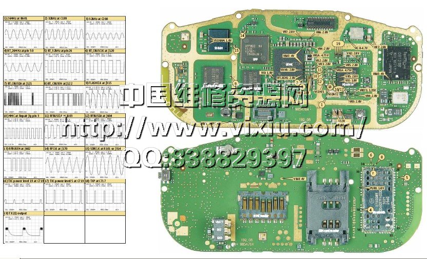
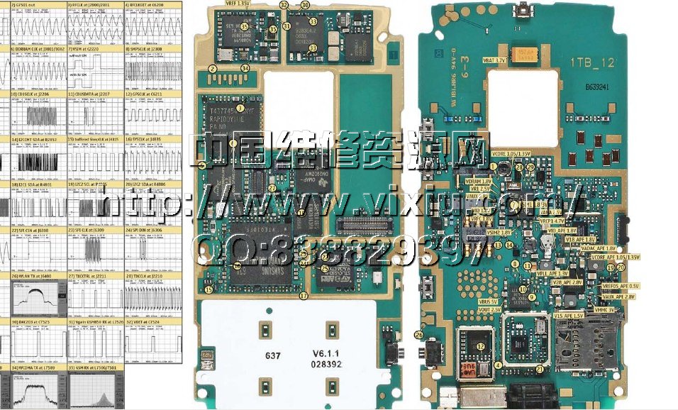
Test points
Receiver test points
Transmitter test points
Synthesizer test points
EGSM900 frequencies
GSM1800 frequencies
GSM1900 frequencies
DC supply voltage sheck
9 System Module
Baseband description
PWB
Environmental Specifications
Technical specifications
Baseband core
Energy management
Power distribution
DC characteristics
Function groups
Battery
Audio
Camera
Vibra
LCD modules
Keypad
Illumination
SIM
FM radio
HALL sensor
Interfaces
RF module description
General specifications of the transceiver
Frequency concept
RF power supply configuration
RF block diagram
Antenna switch (TX/RX switch)
Signal paths
Printed wiring board
10 Schematics
DCT-4 common baseband
System connector, audio
UEME, SIM
UPP, combo memory
FM radio
UI, vibra, keyboard
Flip part, displays, camera
RF part
Signal overview
Component finder
A Differentiation between 900 MHz and 850 MHz (US) versions (RM-76
vs. RM-77)
Differentiation between 900 MHz and 850 MHz (US) versions (RM-76 vs. RM-77)
Glossary
6108(RH-4)
10 - SCHEMATICS
Table of Contents
Title: Top level schematic
Title: Top sheet (2)
Title: DCT4 Common Baseband Schematic (Top level 2)
Title: 5 pin Production Test Pattern
Title: RF top sheet schematic
Title: Mjoelner
Title: Power amplifier
Title: BB RF interface components
Title: DCT4 common BB Schematic (top level)
Title: RH-4 System connector
Title: GSM RF BB interface
Title: RH-4 Audio
Title: MultiGND symbol bypass
Title: GENIO and GPIO connection block
Title: Rohm IR module 1.8V
Title: Testpoints based Ostrich interface
Title: Test and emulator interface
Title: SIM reader
Title: Testpoints for JTAG emulator
Title: DC/DC convertor
Title: RH-4 User interface
Title: Discrete power management
Title: Light filtering
Title: Old power discrete users
Title: UPP 8M implementation
Title: Combo memory 128 +8 Mbit
Title: Discrete decoupling capacitors for UPP
Title: Discrete capacitors for memory without VFlash 1
Title: Empty wing sheet
BACK TO MAIN PAGE
6110(NSE-3)
Schematic Diagrams of UP8
V.14
Block Diagram
Baseband Block Diagram
Power Supply
SIM Connectors
CPU Block
Audio
IR
RF Block
Layout Top
Layout Bottom
V.15
V.16
V.17
MAIN TOC
6111(RM-82)
6120c(RM-243)
6125(RM-178)
6131_6133_6133_6126(RM-115/126)
6150(NSM-1)
UG3MA Schematics
Baseband
COBBA, CCONT, MAD
Power Supply
SIM Connector
CPU
Audio
IR Module
RF Block
RF
UIF
Layout Diagram
Testpoints
MAIN TOC
6151(RM-200)
6170_7270(RM-47/8)
6180(RH-4)
10 - SCHEMATICS
Table of Contents
Title: Top level schematic
Title: Top sheet (2)
Title: DCT4 Common Baseband Schematic (Top level 2)
Title: 5 pin Production Test Pattern
Title: RF top sheet schematic
Title: Mjoelner
Title: Power amplifier
Title: BB RF interface components
Title: DCT4 common BB Schematic (top level)
Title: RH-4 System connector
Title: GSM RF BB interface
Title: RH-4 Audio
Title: MultiGND symbol bypass
Title: GENIO and GPIO connection block
Title: Rohm IR module 1.8V
Title: Testpoints based Ostrich interface
Title: Test and emulator interface
Title: SIM reader
Title: Testpoints for JTAG emulator
Title: DC/DC convertor
Title: RH-4 User interface
Title: Discrete power management
Title: Light filtering
Title: Old power discrete users
Title: UPP 8M implementation
Title: Combo memory 128 +8 Mbit
Title: Discrete decoupling capacitors for UPP
Title: Discrete capacitors for memory without VFlash 1
Title: Empty wing sheet
BACK TO MAIN PAGE
6201
6210(NPE-3)
6220(RH-20)
6230(RH-12/28)
RH-12/RH-28 Top Level, v. 0, ed. 37
RF Top Level, v. 0.0, ed. 59
RX Front End and Antenna Switch, v. 0.0, ed. 75
HELGA
RF9204 Power Amplifier and Power Detection, v. 0.2, ed. 63
BR4.5 Top Level, v. 6.1, ed. 29
BR45 Audio, v. 1.6, ed. 167
Mirage 2 VGA Camera, v. 1.1, Ed. 194
Test and Emulator Interface, v. 2.0, ed. 41
Testpoints for JTAG Emulator, v. 1.3, ed. 12
Testpoints Based Ostrich Interface, v.1.3, ed. 12
Citizen IR Module 1.8V, v. 6.1.8, ed. 55
IR Resistor 1210, v. 0, ed. 6
Key UI, v. 1, ed. 326
Flash Memory 128 Mbit, v. 2.0, ed. 74
Discrete Capacitors for two Memories without VFlash1, v. 1.3, ed.11
Flash Memory 64 Mbit NAND, v. 2.0, ed. 62
Empty Wing Sheet, v. 0, ed. 10
MMC Interface, v. 2.1, ed. 79
UEME Power Management - Dual 1 uF 6V3 Capacitors, v 1.0, ed. 307
UEME ADC Filter Block - BSI, BTEMP and Active PATEMP, v. 1.0
DC_DC for TIKU and VIO, v. 1.7, ed. 75
Light Filtering for Projects using 1uF Caps, v. 1.0
Digital-ASIC-dependent Signal Routing - TikuXX Systems, v. 1.0
32KHz Crystal - Micro Crystal CC4VT2, v. 0, ed. 6
PWR Resistor 1210, v. 0, ed. 4
GSM RF - Baseband Interface, v. 1.3, ed. 64
64Mbit 1V8 SDRAM Memory, v. 1.0, ed. 64
SIM Reader, v. 1.3, ed. 66
System Connector, v. 0.0, ed. 196
Current Measure, v. 0, ed. 18
5 pin Production Test Pattern, v. 2.0, ed. 52
TIKUedge Implementation (GSM)
Discrete Decoupling Capacitors for Tiku, v. 0, ed. 12
TikuEDGE Bus Conversion Sheet, v. 1.2, ed. 102
FM Radio Unit, v. 1.3, ed. 198
Differential Stereo. v. 0.0, ed. 7
Low Power RF Module
GENIO and GPIO Connection Block, v. 0.0, ed. 38
BACK TO MAIN PAGE
6230i(RM-72)
6233(RM-145/123)
6235/6235I/6236I(RM-60)
Top Level
Baseband - Top Level
FM Radio
System Connector
Audio
SIM Card
Key User Interface
UEMEK
Infrared
GPS Top Level
GPS RF
GPS BB
D2800
Camera
Memory
Test and Emulator Interface
RF-BB Interface
RF - Top Level
N7000
PA
UHF Synthesizer
Front End (N7160)
N7100
Component Layout - Top
Component Layout - Bottom
Back to MAIN PAGE
6250(NHM-3)
RF/ BB Connections
Power
CPU
Hagar
Switch
Audio
RX
PLL
Infrared
TX
UI
Layouts
Shields
Back to Main TOC
6260(RM-25)
6255
6255/6255i/6256/6256i (RM-19) Schematics - Main PWB
Baseband - Top
Front End
Audio
N7100 Rx Downconverter
Key UI
System Memory
MMC
SDRAM Memory
PA
RF-BB Interface
RF - Top
SIM Reader
Sharp IR Module
System Connector
UHF Synthesizer
Top Level - Part 1
Top Level - Part 2
UEME
UPP
N7000 Tx Upconverter
FM Radio
J-Tag
Low Power Radio Frequency (LPRF)
6255i and 6256i GPS Schematics - Secondary Display
GPS Top Level
GPS Shield
GPS RF
GPS BB
6255 and 6256 Non-GPS Schematics - Secondary Display
Flex Cable
Flex Interface
Component Layouts and Values - Main PWB
Component Layout - Top
Component Layout - Bottom
Component Values - Top
Component Values - Bottom
6255i and 6256i - Component Layouts and Values - Secondary (UI) PWB
6255i and 6256i Component Layout - Top
6255i and 6256i Component Layout - Bottom
6255i and 6256i Component Values - Top
6255i and 6256i Component Values - Bottom
6255 and 6256 (Non-GPS) Component Layouts and Values - Secondary Display
6255 and 6256 Component Layout - Top
6255 and 6256 Component Layout - Bottom
6255 and 6256 Component Values - Top
6255 and 6256 Component Values - Bottom
Flex Cable Component Layout - Top
Back to MAIN PAGE
6267(RM-210)
6270(RM-56)
6280(RM-78)
6300(RM-217/222)
Service Manual Structure
1 Schematics
AV connector, mini USB, charger jack
RETU, SIM, Audio
TAHVO
RAPGSM, Combo, microSD
FM radio, Bluetooth
User interface
Camera
RF part
Signal overview
Component finder
6305
6310(NPE-4)
6510(NPM-9)
LA5 module Schematic Diagrams
RF& BB
RF
BB Connections
System Connector
Audio Interface
UEM of BB
Light Filtering
Display and Keyboard Interface
Infrared Module
FM Radio
SIM Reader
UPP and decoupling capacitors
Discrete capacitors for UPP
GSM RF-BB Interface
Flash Memory
Discrete capacitors for memory without VFlash1
Test pattern - 5 pin
Layout Diagram of LA5 - top
Layout Diagram of LA5- bottom
Testpoints of LA5
UI Board LU9
Layout Diagram LU9
Return to main TOC
6555(R271/RM-276/RM-289)
6600(NHL-10)
6610-7210(NHL-4)
6630(RM-1)
6670-7610(RH-67/51)
7610-6670板图
6680(RM-36)
6681(RM-57/58)
10 Schematics
Baseband - RF connections
System connector
RETU, SIM, audio
TAHVO
RAP3G, SDRAM, Flash
OMAP, combo memory, camera
Bluetooth
B to B connections
RF part
Component finder
6708(RM-139)
指引
一般维修信息
给维修室工作人员指引的网页
手机器件分解图
零配件清单
维修工具
软件升级
用户信息保存与恢复
拆机步骤介绍(更详细的拆装机演示请参加E时代联盟的在线学习)
示意图快速简单故障排除指引
快速故障排除指引示意图1
快速故障排除指引示意图2
快速故障排除指引示意图3
摄像头功能测试
蓝牙与红外传输功能测试
网络及通话功能测试
6800(NHL-6)
BACK TO MAIN PAGE
7系列(13)
7110(NSE-5)
7200(RH-23)
Top Level
Common BB
System Connector
FM Radio
FM Radio
9 Pin Production Test Pattern
GSM RF - BB Interface
Combo Memory
Empty Wing Sheet
Discrete Capacitors for Memory Without VFlash1
MultiGND Symbol Bypass
IR Module
UI
Discrete Power Management
Light Filtering
DC/DC Converter
For Old Power Discrete Users
UPP 8M Implementation
Discrete Decoupling Capacitors for UPP
Audio
RF Top Level
RF Shields and Vias
RX Front End and Antenna Switch
HELGA
TX
Component Placement Diagram Bottom
Component Placement Diagram Top
Return to Main TOC
7250/7250I(NHL-4J/4JX)
7260(RM-17)
DCT-4 common baseband
System connector, audio
UEME, SIM
UPP, combo memory
FM radio, camera
UI, vibra, keyboard
RF part
Signal overview
Component finder
BACK TO MAIN PAGE
7270(RM-8)
7280(RM-14)
Audio
BTH COST
Top level
Micro BB enginel
RF-BB interface
UEMEK
DC-DC for Tiku
Light filtering
MultiGND
Flash memory
Tiku EDGE
Tiku GPIO and GENIO
FM radio
CBUS
Differential stereo
TEA5761UK
RF top level
Power amplifier and detection
RX front end and antenna switch
Helgo
Micro BB top levely
IR module
MultiGND symbol bypass
5 pin production test pattern
UI
SIM reader
Test and emulator interface
Testpoints based Ostrich interface
Camera
System connector
Current measure
BACK TO MAIN PAGE
7360(RM-127)
7370(RM-70)
7373(RM-209)
7380(RM-111)
7500(RM-249/250)
7600(NMM-3)
Chapter 8 - SCHEMATICS (Me8_20 Version_5 PWB)
Table of Contents
Title: BB + RF Block Diagram
Title: Baseband Block Diagram
Title: USB & System Connector
Title: UEME Display
Title: TIKU, Flash, Bluetooth, Irda, Camera
Title: RF Block Diagram
Title: RF GSM
Title: RF WCDMA
Title: Signal Overview
Title: Component Finder
BACK TO MAIN PAGE
7610(RH-51)
7650(NHL-2NA)
LG4 Schematics & Layout Diagrams
RF-BB connection diagram
System Connector Diagram
Accessories interface diagaram
AEM diagram
Baseband Diagram
BB-RF Interface diagram
CPU Diagram
IR module diagram
RF diagram
Memories diagram
Power Diagram
Audio
UEM Diagram
User Interface Diagram
Parts Placement Diagram LG4
DIM
I1
I8
Testpoints Bottom
Testpoints Top
Values Top
ASM Bottom
ASM Top
Parts List
BACK TO MAIN PAGE
7710(RM-12)
8系列(7)
8210(NSM-3)
RM7L Schematics
RFand BB Connection
Baseband Block Interconnections
Power Supply
CPU
RF
Audio and RFI
IR
UI
RM7L Layout
RM7L Testpoints
BACK TO MAIN PAGE
8250板图
8310(NHM-7)
8600(RM-164)
8800(RM-13/33)
8810(NSE-6)
US8 Schematics
UIF Block Diagram
UIF Circuit Diagram
Baseband Block Diagram
Baseband Circuit Diagram
Power Supply
SIM Connectors
CPU Block
Audio
IR Module
RF Block Diagram
RF Circuit Diagram
Layout of US8
Test points of US8
Test point description
MAIN TOC
8850(NSM-2)
RM7 Layout 19
RF and Baseband Connection
Baseband Block Interconnections
Power
CPU
RF
Audio and RFI
IR
UIF
Layout Diagram
Testpoints
BACK TO MAIN PAGE
RM7 Layout 14
8910(NHM-4)
9系列(6)
9000i(RAE-1N)
PDA
Block Diagram
Power Unit
Serial Interface
MCU and Memory
EMIU
Keyboard Matrix
Memory
Component Layout
BACK TO SCHEMATICS
BACK TO MAIN PAGE
9110(RAE-2)
SCHEMATIC DIAGRAMS ISSUE 2
Block Diagram PDA v.12
Circuit Diagram of UI Flex IF
Circuit Diagram of QWERTY
Circuit Diagram of PDA PWRU
Circuit Diagram of PDA MEM
Circuit Diagram of PDA MCU
Circuit Diagram of PDA B0B0
Circuit Diagrams of PDA HF IF and Earphone
Circuit Diagrams of PDA PLL and IRDA
Circuit Diagrams of PDA Syscon pads and Lid Switch
Test Pads BS1 PDA
Parts Placement of BS 1 PDA v.12
BS 2 Circuit Diagram
Parts Placement Diagrams of BS2
BS8 Block Diagram
Circuit Diagram of GSM RF
Circuit Diagram of CMT Power
Circuit Diagram of BS8 SysCon
Circuit Diagram of CMT CPU
Circuit Diagram of BB Conn
Circuit Diagram of CMT Audio
Parts Placement of BS8
MAIN TOC
9210(RAE-3/5)
9210i(RAE-5)
Schematic Diagrams
/ 2002
AMENDMENT
RECORD
SHEET
Table of Contents
Block Diagram of UL1_07 QWERTY keypad
Block Diagram of UL1_07 CMT keypad
Circuit Diagram Power interface
Circuit Diagram of CMT UI LEDs
Circuit Diagram of PDA backlight
Parts Placement Diagram of UL1:07
Parts Placement Diagram of UL1:07
Block Diagram of KL8_05
Circuit Diagram of System connector
Circuit Diagram of Audio
Circuit Diagram of CPU
Circuit Diagram of PDA
Circuit Diagram of memories
Circuit Diagram of MMC
Circuit Diagram of Power
Circuit Diagram of UIF
Circuit Diagram of RF/BB connector
Circuit Diagram of RF
Parts Placement Diagram KL8_05 1/2
Parts Placement Diagram KL8_05 2/2
Return to main TOC
9300(RAE-6)
9500(RA-2/3)
8 - Schematics
DCT-4 common baseband
UEMK, SIM, Zocus
UPP, Flash
APE overview connection
OMAP, IRDA, MMC
Audio DAC, Audio amplifier
Hinge Camera flex connector, interface
WLAN baseband
WLAN RF
QWERTY keyboard
RF-part
Signal overview Side 1
Signal overview Side 2
Component finder Top side
BACK TO MAIN PAGE
E系列(6)
E50(RM-170/171)
E51(RM-244)
E60(RM-49)
E61(RM-89)
E61i.(RM-227)
E65(RM-208)
E70(RM-10/24)
N系列(17)
N70(RM-84)
N71(RM-67)
N72(RM-180)
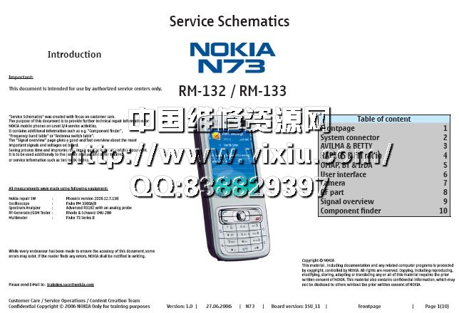
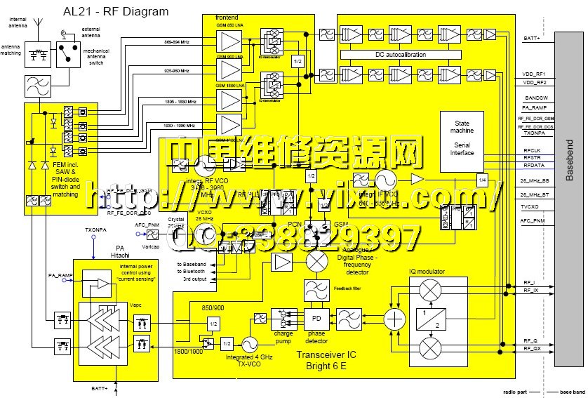
N73(RM-132/133)
N76(RM-135/149)
N770(SU-18)
N77(RM-194)
N80(RM-92)
1MJ_08_Schematics.pdf
1MJ_08a_schdrw__.pdf
/nokia/fa_nmp/groups/R1113_Miro/Unix/product_hw_impl_integr/electronics/PWB/UI/1MJ_08
Miro Rigid UI Connection PWB
N81(RM-179)
N800(RX-34)
N90(RM-42)
N91(RM-43)
N92(RM-100)
N93(RM-55)
N93i(RM-157)
N95(RM-159)
N95(RM-159)
N-GAGE(NEM-4)
Connections between RF and BB modules
NEM-4 BB
UPP_WD2 NEM-4
Power
NEM-4 AUX Power
UEM
Audio
ADSP and FLASH
FM Radio and Audio Codec
Memories
UI
UI
Keypad
Card and USB Interface
Accessory Interface
System Connector
LPRF BT102
Test Interface
GSM BB-RF Interface
Connectors Between RF Modules
Power Amplifier
Mjoelner
Testpoints
Component Placement Diagram Bottom
Component Placement Diagram Top
BACK TO MAIN PAGE
N-GAGE_QD(RH-29)
QD板图


 站内资料搜索